Designing a printed circuit board was once a daunting task, but design automation tools and standard schematics for many common applications have made PCB board design almost commonplace. You don’t even have to own expensive software. We have state of the art schematic capture software and can translate your circuit quickly and efficiently into a printed circuit boards design that follows industry standards and can be manufactured at any production facility.
There are several basic steps to follow if you want a printed circuit board designed. With some basic information in hand, our knowledgeable professionals are ready to design a printed circuit board tailored to your needs.
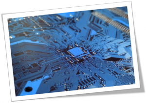
A printed circuit board (or PCB) electrically connects and mechanically supports electrical or electronic components using pads, conductive tracks, and other traits etched from at least one sheet layers of copper laminated onto or between non-conductive substrate’s sheet layers. Generally, the components are soldered onto the printed circuit board to both mechanically fasten and electrically connect with them.
Characteristics of printed circuit boards
Through-hole technology
The first printed circuits made use of through-hole technology, mounting electronic components by leads soldered onto copper traces on one side and inserted through holes from the other side. Board may be more compact double-sided or just single-sided with an unplated component side, with components soldered on both sides.
Surface-mount technology
In surface-mount technology, the components were mechanically redesigned to have small end caps or metal tabs that could be soldered directly on the surfaces of printed circuit boards, instead of wire leads to pass through holes. The component placement on both sides of the board become common, and the components became much smaller, permitting much smaller printed circuit board design assemblies with much higher circuit densities.
Circuit properties of the printed circuit board design
In fast switching radio-frequency circuits the capacitance and inductance of the printed circuit board conductions become substantial circuit elements, often undesired; conversely, they may be utilized as an intentional part of the printed circuit board design, as in antennae, fuses, distributed element filters, and fuses, obviating the requirement for more discrete components.
Materials
- RoHS compliant PCB: In consumer items, the European Union bans the use of lead, among other heavy metals. If PCBs are to be sold in the EU, they must comply with RoHS (or restriction of hazardous substances).
- Laminates: Laminates are formed by curing under temperature layers and pressure of paper or cloth with thermoset resin to formulate an integral final piece of uniform thickness. The differences in resin percentage, cloth thickness, and cloth weaves are used to accomplish the desired final dielectric characteristics and thickness.
- Key substrate parameters: Usually, the circuit board substrates are composite dielectric materials. The composites comprise a reinforcement (sometimes nonwoven, usually a woven, glass fibers, sometimes even paper), a matrix (usually an epoxy resin) and in certain cases, a filler is added to the resin (for instance, ceramics; dielectric constant may be increased by using titanate ceramics).
- Common substrates: The materials often encountered are FR-2, phenolic cotton paper, or phenolic paper; FR-4 a woven fiberglass cloth impregnated with epoxy resin; aluminum; and flexible substrates, can be laminated to a thin stiffener or can be a standalone copper-clad foil.
- Copper thickness: the Copper thickness of PCBs may be directly specified or as the weight of copper per area, which is far easier to measure. Heavy copper layers are used to help dissipate heat and for high current.
- Safety certification (US): The component safety requirements are covered by the Safety Standard UL 796 for printed wiring boards for use as components in appliances or devices. The testing analyzes features such as live electrical parts, heat deflection, electrical tracking, maximum operating temperature, and flammability.